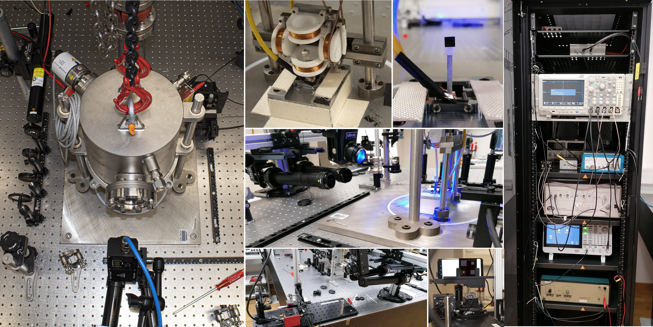
Experimental Facilities
The experimental facilities of the Mechanics & Materials Lab are housed primarily on the J and H floors of the CLA building on ETH's city center campus. We perform fundamental experiments to study mechanical problems ranging from the static and dynamic behavior of architected (meta-)materials to multi-physical coupling phenomena in ferroelectric ceramics. A wide range of both custom-built and commercial instrumentation allows us to probe these complex problems across length and time scales. Experiments are designed with the goal of discovering new phenomena, measurement of fundamental processes in materials as well as validation of computational material models developed within the lab.

1. Broadband Electromechanical Spectroscopy (BES)
BES is an experimental technique designed and developed by Prof. Kochmann's team to study electromechanical phenomena in bulk ferroelectric materials. The experiment allows application of large-amplitude arbitrary static and dynamic electric fields to millimeter-scale samples with a cantilever beam geometry. The experimental setup has the capability of applying voltages up to 10 kV. The resulting volume-averaged polarization is measured using custom-built circuits with microsecond time resolution. The polarization-coupled mechanical strains are measured in-situ, with micrometer spatial and microsecond temporal resolution, using a laser point position-sensing detector and a 3D Digital Image Correlation (DIC) system simultaneously. In addition, the BES enables the application of transient bending and torsional vibrations during electrical cycling, thus allowing us to measure dynamic viscoelastic properties during the evolution of electrical polarization.
Following is a brief description of the essential components of the BES setup in the Mechanics & Materials Lab.
High Voltage amplifier
A Trek (model: 10/10B-HS) amplifier is used to apply large voltages up to 10 kV to bulk ferroelectric ceramics and crystals.
Output voltage: 0 - ±10 kV
Output current: 0 - ±10 mA DC or 40 mA peak AC
Slew rate: > 700 V/μs
Bandwidth: 20 kHz
Gain: 1000 V/V fixed
Sawyer-Tower circuit
The Sawyer-Tower circuit is used to measure the time-resolved volume-averaged polarization evolution in bulk ferroelectric samples in situ. Our circuits are built in-house to allow for polarization measurements at large applied fields over time scales ranging from nanoseconds to minutes.
Helmholtz coils
Helmholtz coils are used to apply small-amplitude cyclic mechanical loads to the ferroelectric samples during the application of electric loads. This allows us to probe the viscoelastic properties of these ceramics as a function of polarization over a wide range of frequencies.
Position-sensing detector
The mechanical deformation of samples is measured using two simultaneous measurement techniques. Using a 5 mW Helium-Neon CW laser (LASOS Lasertechnik GmBH) and position-sensing detector (Thorlabs PDP90A) with resolutions down to 750 nm, we measure the deflection of the end of the cantilever beam samples due to both polarization evolution and mechanical vibrations.
Lock-in amplifier
We use a Zurich Instruments MFLI lock-in amplifier to measure small-amplitude frequency locked signals from the deflection sensor.
Frequency range: 500 kHz
Sampling rate: 60 MHz
Resolution: 16 bits
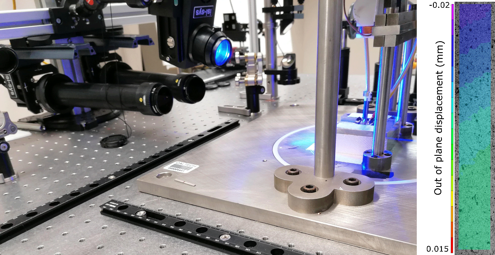
3D Digital Image Correlation (DIC)
We use high-resolution cameras (Basler Ace 12 Mpx, 30 Hz max frame rate) in a stereo configuration along with the Vic-3D Digital Image Correlation software (provided by isi-sys GmbH) to measure the evolution of 3D strains and displacements on the surface of our sample during dynamic electromechanical loading.
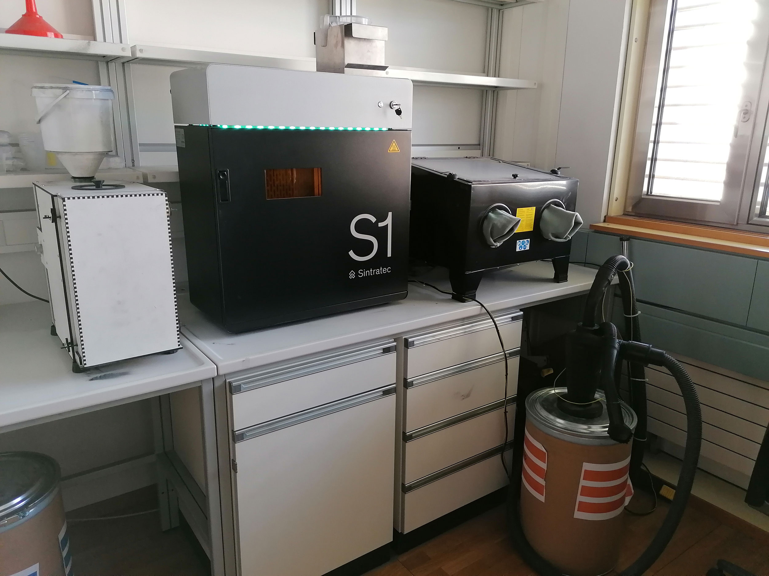
2. 3D printer
Our Sintratec S1 3D-printer is housed in the CLA labs of the Mechanics & Materials Lab. This pirnter uses a selective laser sintering (SLS) technique to print 3D structures. Two types of materials can be printed at present: a thermoplastic elastomer (commercial name: TPE) and polyamide (nylon) (commercial name: PA12).
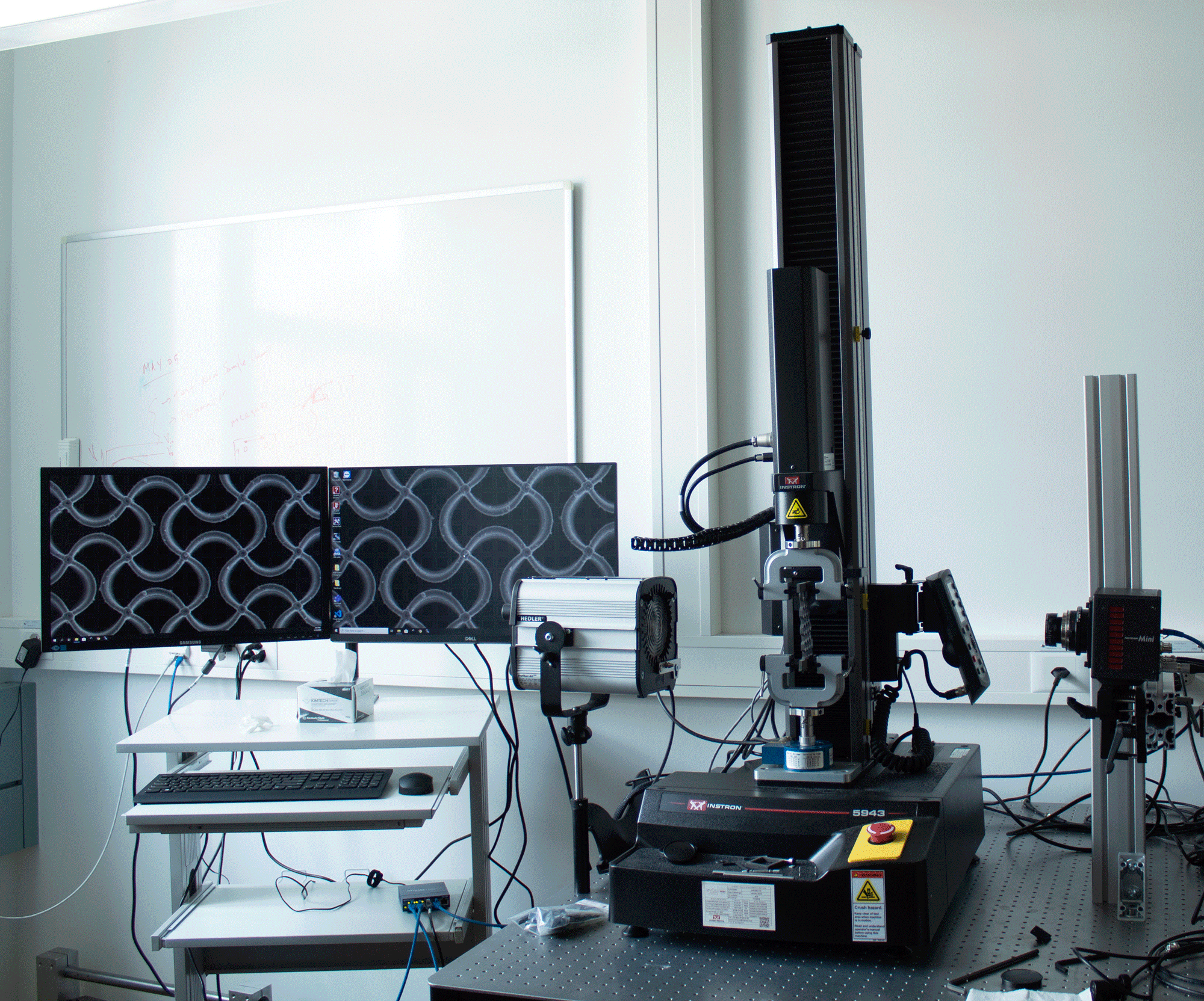
3. Instron quasistatic testing
We use an Instron 5940 series tabletop frame for quasistatic mechanical testing. The frame is equipped with a torsion add-on for multi-axial experiments.
Cross-head velocity: 0.05-2500 mm/min
Rotation speed: 60 rpm
Force transducer: 450 N, 20 Nm multiaxial load cell, 1 kN axial load cell
4. Imaging technology
Cameras: The Mechanics & Materials Lab houses a variety of cameras along with different optical lens systems for low and high speed imaging.
High-resolution cameras
Model: Basler acA 4112- 30μm
Pixel size: 3.45 μm x 3.45 μm
Resolution: 4096 x 3000 px
Max. fps: 30 fps
High-speed cameras
Model: Photron AX200
Pixel size: 20 μm x 20 μm
Max. resolution: 1024 x 1024 px
Frame rate: 6400 fps at max. resolution
Light sources
Hedler LED1000 (for high speed imaging): up to 1 kW
Blue-X-Focus: 200W @ 100 Hz, down to 1 μs exposure
Analysis software
Besides using Vic3D Digital Image Correlation (DIC) software, MMOptiLab is our repository for the in-house development of image analysis codes. Calculating displacement/velocity fields from the complex yet ordered “mesostructures” of truss-based architectured metamaterials using conventional DIC methods is non-trivial. We therefore develop analysis algorithms for this specific class of metamaterials under static and dynamic loads with high spatial and temporal resolutions.
5. Shared facilities and collaborations
3D printing
We have access to various shared 3D printing facilities in the department (including a Connex 500 multi-material printer and a Fortus 400mc polycarbonate printer).
Sample preparation
We use sample preparation equipment, specifically for mechanical polishing and sputter deposition of thin film electrodes (on ferroelectric samples) at the ScopeM microscopy user facility on the Hönggerberg campus of ETH
Scanning Electron Microscopy (ScopeM)
The Mechanics & Materials Lab is a registered user of the ScopeM microscopy user facility on the Hönggerberg campus of ETHZ. We use the FEI Quanta 200F Scanning Electron Microscope (SEM) for imaging and Electron Back-Scatter Diffraction (EBSD) characterization of ferroelectric ceramics.
Collaboration(s)
We collaborate with the Laboratory for Multifunctional Ferroic Materials research group housed in the materials science department (D-MATL) of ETH Zürich to image spatially-resolved polarized domains in ferroelectric samples using Scanning Probe Microscopy techniques. We further collaborate, among others, with external page Prof. Julia R. Greer and team at Caltech and external page Prof. Carlos Portela at MIT, who perform small-scale metamaterial fabrication and characterization, external page Prof. Chiara Daraio at Caltech on nonlinear metamaterials, and external page Profs. Katia Bertoldi and external page Jennifer Lewis at Harvard University on the design of reconfigurable metamaterials.